Most fresh paper: PDF
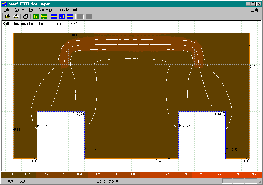
Here are 3D-MLSI slides. The slides are .BMP screenshots of current colour maps with streamlines. For problems discussion, see SDE CAD tools, Inductance Rodeo Results.
Here is manual: PDF.
Here is student version of the program with examples (manual included). It is compiled for W32.
The dimensions of the typical superconductor devices are small (SDE CAD tools, Inductance Rodeo Results). The total thickness of RSFQ layouts is less then 1 µm, the thickness of the layers of metallization and embedding media are 0.1-0.3µm. The London penetration depth can be less or can be compared with the thickness of the conducting layers. The width and length of the conductors in each layer are significantly larger then thickness of the layers and the total thickens of the structure. The width of conductors, for example, in HYPRES technology can not be less 2µm.
Recently some programs for the inductance extraction of typical microelectronic structures were developed. The 2D transmission line problem was considered in [1] and [3]. In details extraction of transmission line inductances is presented here (the program LL) or here (the program TLZ).
Different 2D approaches, exploiting the presence of total ground plane and assumption of 2D structure of magnetic field, were presented in [4] and [5] (the programs LMETER and INDEX). Though these programs are fast and can be applied for large layouts with tens of Josephson junctions, they do not allow investigating important 3D effects, which are of great interest in new low-Tc and high-Tc cryoelectronic circuits.
As the importance of real 3D simulations was evident, the programs [6], [7], [8], [9], [10], [11], [12] were developed as attempts to solve the problem. All these programs except [9] where the analogy with the normal conductor is used, exploit the same well known for normal conductors PEEC technique. In clear way this technique is presented in [13] and [12]. In this approach certain net of wires simulates the conductors. The currents in the wires need to be defined by use of Maxwell and London equations. Typically, the minimization of the total free energy for this purpose is used. The main disadvantages of this approach are low precision and great time and memory requirements [10]. As result on practice usually it is necessary to reduce the number of degrees of freedom and the ground plane is simulated by mirror image method [10] In this case important effects of the penetration of the magnetic field into the groundplane are lost. The error of mirror image method can be about 30%.
The reasons of the poor effectiveness of the existing 3D electromagnetic simulators for superconductor circuits are the complexity of the problem itself, the low order of convergence of the numerical technique and ignoring the fact of planarity of the problem.
In this work, we try to overcome the difficulties described above. The work was performed as the development of the investigations [14].
We start our analysis from general steady Maxwell and London equations. Then we simplify the equations under the assumptions of the smallness of total height of the circuit compared with the lateral sizes of the circuit. It is shown that only z- component of vector London equations is important for our analysis.
As the next step we introduce the stream function (T-function, or vector potential with one component only). It is scalar potential representation for the current density. The full and correct setting of boundary value problem for this potential representation is then derived. The problem contains integro-differential equation with hypersingular integral operator and boundary conditions. This approach in rigorous but clear and in very simple form contain:
The finite thickness of the layers with conductors is taking into account by use of modified singular kernels of integral operators.
The structure of current distribution is completely defined by boundary conditions just as for Laplace equation. It is not necessary to introduce the filament excitation currents as PEEC technique needs.
The matrix of self and mutual inductances is defined on the base of this boundary value problem and the expression for the full energy of the system. This matrix is exactly "physical" matrix of self and mutual inductances. This matrix allows calculating fluxoids for holes and terminal currents as was proved in [14] and WSL.
As we could reduce the problem of finite thickness of conducting layers to simple modification of the kernels of the integral operators, the equations we need to solve are very close to the equations in [14] and WSL. Therefore our numerical method is the method of in [14] with some improvements.
This numerical technique is based on the triangulation of the conductors and the linear finite element method on the triangular meshes. In this case circulating currents with piecewise-constant density simulates the density of current. The flexibility of the triangular mesh and improved accuracy of approximation of the current density leads for better effectiveness of our numerical technique.
The numerical approach is proved and leads to the system of linear equations with symmetric positively definite dense matrix. The inductance matrix is calculated by use of sequence of problems for current density. The system of linear equations of finite element method is solved by use of Cholesky decomposition.
Our program does not contain limitations on the form of the conductors. But terminals can be posed only on the external boundary of the conductors. In other words, holes can not contain terminals. This limitation is intrinsic to the stream function technique. In most cases the existing version of the program can be easily applied to the problems with terminals in the holes by use of performing narrow cuts from hole to the external boundary or by calculating partial inductances.
The program contains triangular mesh generator based on one of the modern and most effective techniques [15]. The mesh generator contains the tools for mesh refinement [16].
The program is written on C++ and contain preprocessor and computation module. The program is platform independent and can be compiled for WINDOWS and UNIX.
Input layouts in form of self or DXC format can be viewed by WINDOWS program WPM. This program is WINDOWS shell for all other programs of other modules of 3D-MLSI.
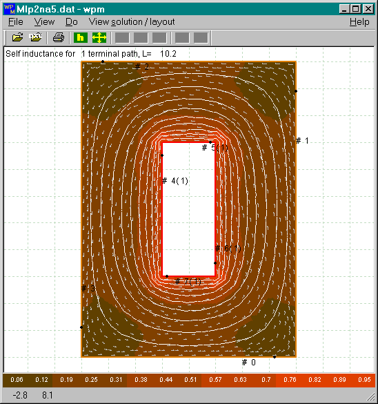
The program WPM allows to view results of calculations. The current density is presented by colour maps. The direction of the current is presented by stream lines and vanes (arrows). Here is the screenshot for simple problem:
Click here to look on the input file.
Except layout configuration it is sometimes necessary to point current loops for inductance calculation. For this purpose we use equivalent circuit of the layout. Current loops are associated with basic loops in the circuit. Then inductances in the equivalent circuit can be founded with help of postprocessing procedure written for MAPLE. This technique is necessary for analysis of complicated circuits. For simple problems current loops are evident.
The first example is low L (test #1) and high L (test #2) from [17] and Inductance Rodeo Results. The cross-section of strip and groundplane is presented on the picture:
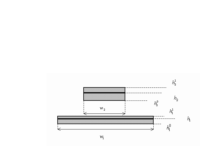
The length of the strips is large enough for terminal current distribution has no influence on the results.
We calculated more precious, then 3D-MLSI, values of inductances by use of our program LL. The results are presented in the table:
| Ll(0.773)pH/10mm | Lh(1.93)pH/10mm | Remarks | |
| w1 | 10mm | 6mm | |
| w2 | 5mm | 3mm | |
| h10 | -0.1 | -0.1 | |
| h11 | 0.0 | 0.0 | |
| h20 | 0.15 | 0.5 | |
| h21 | 0.3 | 0.8 | |
| l | 40 | 20 | |
| L(*)(1) | 0.64(17%) | 1.86(3.6%) | h1 = h11, h2 = h20 |
| L(*)(2) | 0.74(4%) | 1.98(2.6%) | h1 = 0.5(h00+h01), h2 = h20 |
| L(*)(3) | 0.79(2.5%) | 2.19(13.5%) | h1 = h11, h2 = 0.5(h20+h21) |
| L(**) | 0.77(0.1%) | 1.97(2.2%) | |
| N | 693 | 227 | |
| t(*) sec | 126 | 26 | |
| t(**) sec | 181 | 33 | |
| tprepr sec | 19 | 5 |
Table 1: Strip line of length l over groundplane, l = 0.09mm. N - dimension of main matrix, t - time of computations, tprepr - triangular mesh preprocessor time. Inductance per 10mm. (*)-infinitely thin sheet model for height of layer hi, (**)-finite thickness model.
Both variants of mathematical model show good results, but it is necessary to fit height of infinitely thin layers.
In contrast with [10] and Inductance Rodeo Results, we easily do not use mirror reflection method for groundplane. Instead, we present the results for real ground plane calculations. As follows from calculations Inductance Rodeo Results, the error of mirror method can be 28% for low L strip and 15% for high L strip.
For method (*) (infinitely thin sheets) M0 layer is simulated by its upper surface, M1 layer is simulated by its middle surface and M2 layer is simulated by its lower surface.
The results for two different values of London penetration depth are presented in the table 2.
| L11/10mm | L12/10mm | L22/10mm | |
| l = 0.09mm | |||
| 2D | 0.772 | 0.63 | 1.71 |
| (*) | 0.797(3.3%) | 0.635(0.8%) | 1.689(1.2%) |
| (**) | 0.763(1.2%) | 0.657(4.2%) | 1.768(3.4%) |
| l = 0.3mm | |||
| 2D | 3.424 | 1.91 | 4.3 |
| (*) | 3.495(2%) | 1.98(3.7%) | 4.29(0.2%) |
| (**) | 3.47(1.3%) | 1.98(3.7%) | 4.34(0.8%) |
Table 2: M1 and M2 strip lines over groundplane.
The program show good accuracy for three-layer structures.
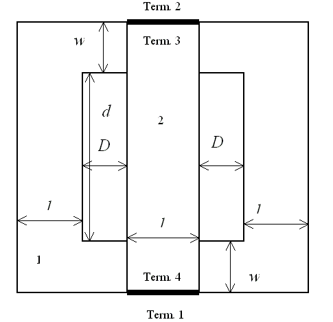
All test examples presented in Inductance Rodeo Results can be calculated not only by 3D but also by 2D program LMETER. Let us consider completely 3D open structure, a strip over a hole. This circuit with all dimensions is presented on the picture:
Such circuit for case of long holes can be modelled by 2D transmission line problem. This approach is presented in [2]. We made calculations for some examples from [2] and found results in good agreement. But short holes, the real 3D problem, as far as we know were not considered yet.
We performed some calculations for the parameters of HYPRES technology process. The thickness of groundplane was 0.1µm, thickness of first metallization layer (strip) 0.2µm, the thickness of dielectric between them 0.15µm, London penetration depth 0.09µm, l=5µm, D=l/2 and 2w+d=4l (see picture above).
In our calculations, L11 is the self inductance of the hole, L22 is the self inductance of the strip, and L12 is mutual inductance of strip and hole.
If the hole contain zero fluxoid, then the next expression for the inductance L of the strip can be derived:
The results of calculations for model of conducting layers of finite thickness and for different values of parameter d are presented on the next graphic:
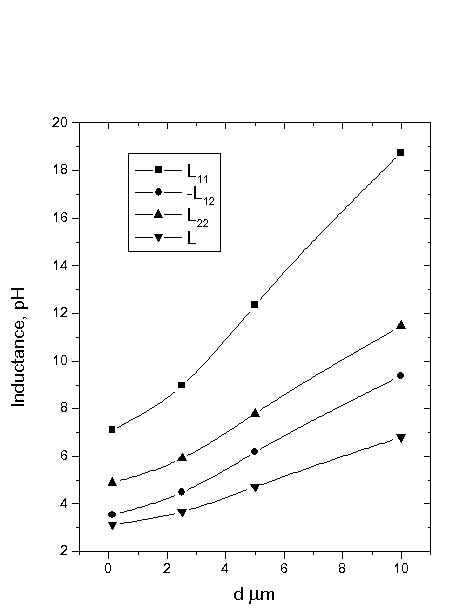
The limiting values of L and L22 for d=0 does not coincide with the inductances from Table 1 (first example). The reason is that the hole tends to cut and current in groundplane need to flow around it.
Other results of inductance calculations with 3D-MLSI (old version of this program called ML) are presented in SDE CAD tools, Inductance Rodeo Results. In same cases there is large difference between results, up to 28%. This fact can be explained by different methods for groundplane simulation. Typical approach is to use mirror image method. In this case no degrees of freedom are used for groundplane representation and calculations are significantly faster. But the magnetic field penetration is omitted and ground plane inductance part is not calculated preciously. In contrast with this approach our program simulate ground plane directly and accurately. Nevertheless due to new numerical technique it is faster then other programs tested in SDE CAD tools, Inductance Rodeo Results and [17]
1. W. H. Chang, "Numerical calculation of the inductances of a multi- superconductor Transmission Line System," IEEE Trans. Magn. 1981. vol. 17. N1. P. 764-766.
2. W. H. Chang, "Measurement and calculation of Josephson junction device inductances," J. Appl. Phys., 1981, v. 52, N3, pp. 1417-1426.
3. M. M. Khapaev, "Extraction of inductances of a multi-superconductor transmission line," Supercond. Sci. Technol., 1996, vol. 9, pp. 729-733.
4. P. H. Xiao et al., "INDEX: an inductor extractor for superconducting circuits'" IEEE Trans. Appl. Superconductivity, 1993, March, v.3, 2629-2632.
5. P. I. Bunyk, S. V. Rylov, "Automated Calculation of Mutual Inductance matrices of multilayer superconductor integrated circuits," Ext. Abs. ISEC'93, p.62, 1993
6. M. Hosoya et al., "Extrapolated boundary element method for three-dimensional inductance calculation," J. Comp. Phys., 1988, v. 74, pp. 94-109.
7. M. Hosoya et al., "Inductance calculation system for superconducting circuits," IEEE Trans. Magn., 1989, v.25, pp. 1111-1114.
8. G. Hildebrandt, F. H. Uhlmann, "Inductance calculation for integrated superconducting structures by minimizing free energy," IEEE Trans. Appl. Superconductivity, 1995, June, v.5, No.2, 2766-2769.
9. Z. Du., S. R. Whiteley, T. Van Duzer, "Inductance Calculation of 3D Superconducting Structures," Ext. Abs. ISEC'97, Berlin, 1997, pp. 293-295.
10. B. Guan, M. J. Wengler, P. Rott, M. J. Feldman, "The inductance estimation for complicated superconducting thin film structures with a finite segment method," IEEE Trans. Appl. Superconductivity, 1997, June, v.7, No.2, .
11. T. Nakazato, Y. Okabe, "Inductance computation of Microscopic Superconducting Loop," IEEE Trans. Appl. Superconductivity, 1997, June, v.7, No.2, 3626-3629.
12. M. Kamon, M. J. Tsuk, J. K White, "FastHenry: a multipole-accelerated 3-D inductance extraction program," IEEE Trans. Microwave Theory and Techn., September 1994, v. 42, pp. 1750-1758.
13. P. A. Brennan, N. Raver, A. E. Ruehli, "Three-dimensional inductance computations with partial element equivalent circuits," IBM J. Res. Develop., November 1979, v. 23, N. 6, pp. 661-668.
14. M. M., Khapaev, "Extraction of inductances of plane thin film superconducting circuits," Supercond. Sci. Technol., 1997, vol. 10, pp. 389-394.
15. S. H. Lo, "Delaunay Triangulation of Non-Convex Planar Domains," Int. J. Numer. Meth. Eng. 1989. vol.28, 2695-2707.
16. W. H. Frey, "Selective Refinement: a New Strategy for Automatic Node Placement in Graded Triangular Meshes," Int. J. Numer. Meth. Eng. 1987. vol.24, 2183-2200.
16.K. Gaj, Q. P. Herr, V. Adler, A. Krasniewski, E. G. Friedman, M. J. Feldman,"Tools for the Computer-Aided Design of Multigigahertz Superconducting Digital Circuits," IEEE Trans. Appl. Superconductivity, 1999, vol. 9, pp. 18-38, March 1999.